
Intel's gamble: more factories serving competitors' chips
Focus. The push to open up their plants to third-party production
also to boost business. Challenge on innovation and large investments
6' min read
Le ultime da Radiocor
***Banco Bpm: da Credit Agricole nessuna richiesta a Bce di superare il 30%
Borsa: il caso Samsung agita i listini, a Milano (-0,9%) tonfo di St e Prysmian
***Trasporti: Urso, attivato Garante prezzi per aumento anomalo biglietti aerei
6' min read
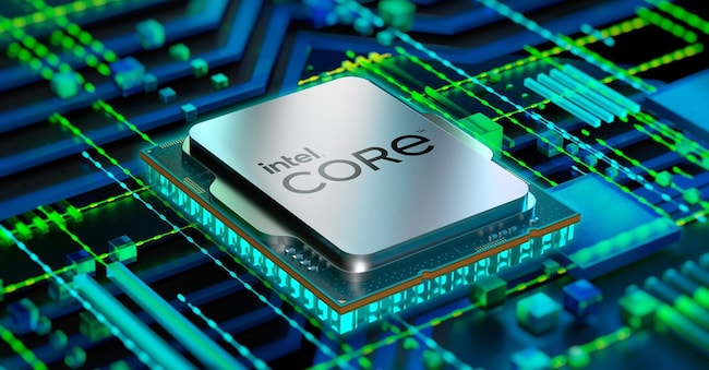
IDM 2.0. That is: Integrated design manufacturer 2.0. This is the strategy initiated a few years ago by Intel and in respect of which, at the end of last February, the group provided important updates. The project, on closer inspection, is at the heart of the re-launch of the Santa Clara microprocessor company. A business rethink that, in order to be better understood, requires a reminder of the group's corporate purpose.
The multinational company is an integrated chip manufacturer. That is, it carries out a large part of the three main phases of semiconductor construction: the design of the chip architecture; the production of the chip on the wafer (essentially by ultraviolet light photolithography); assembly (in plastic or ceramic containers); and testing. All the steps described were historically conducted on Intel's own solutions. Now, however, and this is the main point of IDM 2.0, the group's foundries (factories) are increasingly opening up to third-party production. The company has created an ad-hoc division - renamed Intel foundry a few days ago - to, on the one hand, support the project; and, on the other, underline its objectives. Which are several. First and foremost is growth in the foundry sector. This, according to Statista, is currently dominated by Tsmc (60.2% market share). Then, well behind it, are the likes of Global Foundries (9.9%) and Umc (6.6%). Intel, for its part, boasts a market share of less than 2%. Well: the aim, by 2030, is to become the second global player after the Taiwanese group.
The packaging
.The goal is very - for some too - ambitious. From which it is logical to ask: what cards does Intel intend to play? One theme, emphasised by CEO Pat Gelsinger himself, is packaging (assembly) and advanced testing. This phase of chip production has become crucial. A few years ago it was worth about 15 per cent of the production costs in the most sophisticated processors (mainly used in AI). Now, however, it weighs 35-40% of the overall burden. It is clear, therefore, that on the one hand Intel's experience on this front is an advantage; and on the other, it is not surprising that, just last January, the company started up the Fab 9 in Rio Rancho, New Mexico. A plant - precisely - aimed at the production of advanced packaging technologies.
High-Tech Manufacturing
.But it is not just a question of assembly or testing. The technological challenge, essential to attract customers, is in the production itself. In general, the semiconductor industry is focused on continuous miniaturisation. A context in which the nanometre (one billionth of a metre) is used as a unit of measurement, typically referring to the gate size of the transistor. The smaller this becomes, the more transistors can be inserted into the chip, increasing its computing power. Well: Intel, at its meeting last February, first confirmed the approach - announced about three years ago - of the so-called 5N4y.i.e.: five new production processes in four years. Then he indicated that the programme will expand - by 2027 - with the Intel 14A process. In other words: it will lead to the production of transistors with a 14 Angstron gate, or rather 1.4 nanometres. In the shorter term instead - in 2024 - the 2 nanometre process is planned, and - between 2024 and 2025 - the 1.8 nanometre process. Beyond the individual processes and numbers, it is clear that miniaturisation - together with reliability - is a key element for the success of Intel's strategy. A difficult technological challenge that is played out on the same reduction of energy consumption. A front where the group has begun to exploit PowerVia. A technology which, by having the power supply arrive from the rear of the wafer - instead of the front -, makes it possible to make the chip's energy use more efficient.
That greater efficiency that - and herein lies another objective of the Intel Foundry strategy - is sought in the company's various intramural divisions. An example? The design of the chip architecture. "When,' explains Alessandro Piva, director of PoliMi's AI Observatory, 'the various internal areas, which no longer have exclusive rights to the foundry, are put in competition with external companies, they are forced to improve the quality and quantity of their output.


